Optical Computing Surges as AI Data Centers Confront Power Limits
As AI inference strains global power grids, optical computing startups attract $2.22 billion to challenge silicon with light-speed energy efficiency.
EXECUTIVE BRIEF // KEY TAKEAWAYS
As AI inference strains global power grids, optical computing startups attract $2.22 billion to challenge silicon with light-speed energy efficiency.
NEW YORK — A severe power bottleneck across global data centers running artificial intelligence workloads is driving a commercial revival of optical computing, propelling sector valuations to $2.22 billion as startups and researchers race to replace electrical circuits with light.
The sudden influx of capital—surging from $400 million in 2022, according to a report published by IEEE Spectrum—signals growing industry recognition that conventional silicon graphics processing units face physical energy ceilings during AI inference. With server clusters consuming massive amounts of electricity to process queries for generative models, enterprise operators and semiconductor designers are exploring photonics to bypass electronic resistance, seeking order-of-magnitude reductions in energy expenditure and operating costs.
Reviving Goodman’s Model Amid Power Bottlenecks
While the concept of computing with photons dates back more than 70 years, commercial viability remained elusive until explosive demand for AI inference collided with power grid limits. At the operational heart of modern neural networks lies vector-matrix multiplication, an arithmetic calculation executed billions of times per second. In standard electronics, calculating the product of a vector of length N and an N-by-N matrix requires N-squared distinct operations, each dissipating thermal energy. By contrast, optical architectures pass light through an optical attenuator or modulator passively, requiring power primarily to encode the inputs and read the outputs, scaling energy expenditure linearly with N.
This fundamental physics advantage has ignited renewed interest across academic and venture corridors. In 1978, optical pioneer Joseph W. Goodman demonstrated matrix multiplication using light-emitting diodes, lenses, and an attenuator. Today, modern micro-fabrication and laser systems have turned that laboratory concept into a scalable engineering proposition.
“Most of the interest in [photonics] is driven by the fact that AI inference has literally become limited by power, and in a rather striking manner,” said Peter McMahon, an associate professor of applied and engineering physics at Cornell University who has researched optical computing for more than a decade.
In 2022, a Cornell research team led by McMahon demonstrated an optical neural network consuming approximately 2.5 x 10^-19 joules per multiplication—equivalent to less than one photon of energy. Standard digital computers, by comparison, consume between 10^-14 and 10^-12 joules per multiply operation, implying a theoretical efficiency gain of up to 100,000 times. However, McMahon cautioned that data encoding overhead and Amdahl’s law temper real-world performance gains, noting that optical systems generally require vector lengths between 1,000 and 10,000 elements before overcoming the energy cost of converting electrical data into light.
Architectural Divide: Free-Space Versus Integrated Silicon Photonics
Commercialization efforts in the United States, Britain, Germany, China, and Israel are currently bifurcated into two distinct design philosophies: free-space propagation and integrated silicon photonics.
In the free-space camp, Oxford-based startup Lumai is implementing programmable spatial light modulators through open air to bypass waveguide losses. Lumai is targeting the computationally intensive prefill phase of inference, in which prompt tokens are ingested into memory. Head of product Phillip Burr stated that the startup’s Iris Nova server, scheduled for evaluation in April 2026, serves as a proof of concept, with its subsequent Iris Aura server aimed at running prefill workloads using approximately one-tenth the power of a standard GPU.
In Austin, Texas, hardware developer Neurophos is pursuing free-space manipulation at sub-wavelength scales using engineered metamaterials. Patrick Bowen, chief executive of Neurophos, noted that conventional silicon photonic modulators can span two millimeters, restricting on-chip compute density relative to leading foundries such as Taiwan Semiconductor Manufacturing Co. Bowen’s team developed micrometer-scale metamaterial modulators that switch over 10,000 times faster than liquid-crystal displays, packaging one million modulators onto a five-millimeter chip. Neurophos plans to deliver commercial server racks in 2028, claiming performance targets 50 times faster and 35 times more energy efficient than Nvidia Corp.’s Blackwell B200 accelerator.
Conversely, competitors are turning to integrated silicon photonics, trading the three-dimensional scaling of free space for the established high-volume manufacturing lines of traditional semiconductor foundries.
“There is a good reason that free-space optics are usually limited to 1,000 units a year,” said Michael Förtsch, chief executive and founder of Stuttgart-based Q.ANT. “Semiconductor-manufacturable integrated photonic circuits are at this point way more promising to reach volume production.”
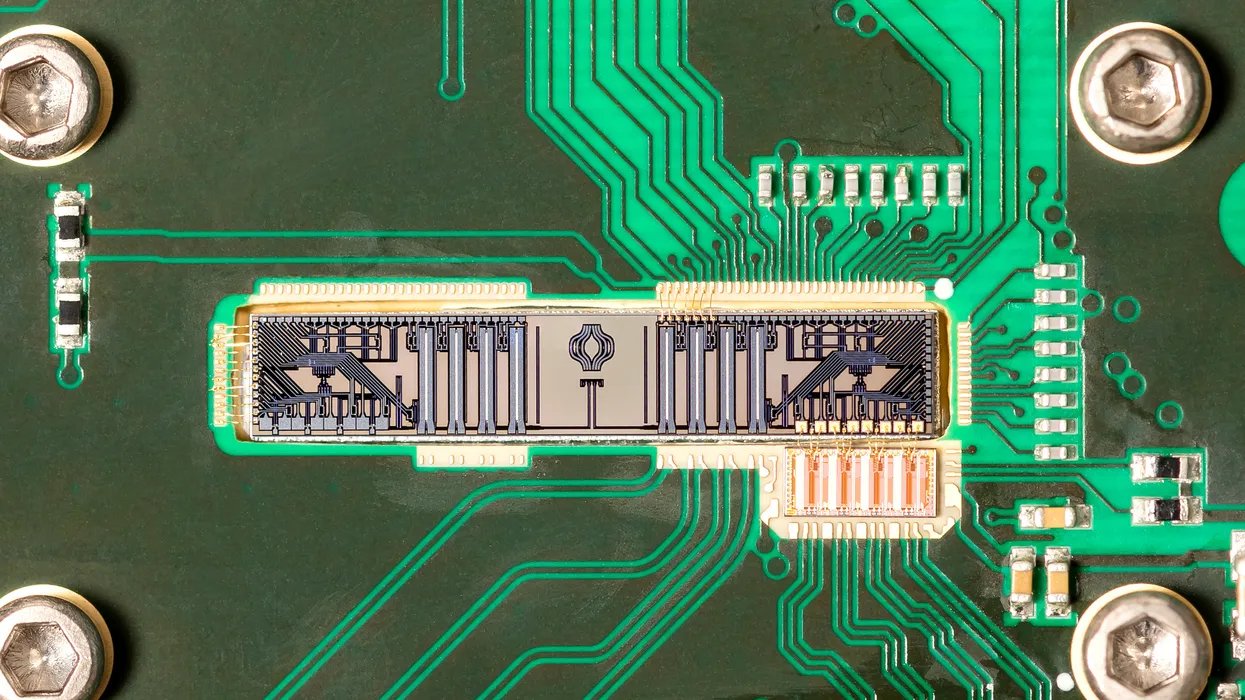
Q.ANT utilizes serialized light pulses traveling through Mach-Zehnder interferometers on-chip, deploying its Native Processing Server across research hubs including the Leibniz Supercomputing Centre and the Jülich Supercomputing Centre, alongside a commercial deployment with European cloud host Ionos. In China, Shanghai-based Lightelligence demonstrated its PACE2 integrated optical processor, executing 128-by-128 matrix multiplications at a one-gigahertz clock rate with three-nanosecond latency—two orders of magnitude faster than conventional silicon.
Alternative Architectures and Heterogeneous Data Center Roadmaps
Beyond traditional vector-matrix algebra, optical hardware developers are targeting mathematical operations where photons exhibit native computational advantages over digital logic gates.
Operations such as Fourier transforms can be calculated almost instantaneously using single passive optical elements rather than hundreds of electronic transistors. Leeds-based Optalysys is integrating on-chip Fourier transform components directly into data center networking fabrics. Founder and chief product officer Nick New noted that embedding passive optical processing directly along optical interconnects addresses the memory-bound decode phase of AI workloads without adding thermal load. In Tel Aviv, startup LightSolver developed a cavity-based laser processing unit that uses stimulated photons bouncing through a gain medium to solve complex differential equations 40 to 80,000 times faster than GPUs in emulation trials.
Despite these technological milestones, industry analysts emphasize that optical computing faces steep adoption hurdles, primarily centered on digital-to-analog conversion overhead and software inertia. Logan Wright, an assistant professor of applied physics at Yale University, observed that machine learning frameworks remain aggressively optimized for graphics processing units. However, co-packaged optics initiatives backed by major chipmakers like Nvidia and TSMC are expected to establish the packaging infrastructure necessary for photonics to penetrate hyperscale facilities.
Rather than wholesale replacement of silicon processors, industry executives anticipate a hybrid computing topology. Förtsch projected that future enterprise infrastructure will rely on heterogeneous architectures, deploying central processing units for system management, graphics processors for generalized routines, and photonic processing units to shoulder power-intensive linear algebra and wave mechanics.