NAED Unveils High-Throughput 4.6 GW Perovskite-Silicon Tandem Line
NAED Energy Holding details its PV-1 manufacturing line, achieving 16,000 wafers per hour to scale perovskite-silicon tandem cells to 4.6 GW annual capacity.
EXECUTIVE BRIEF // KEY TAKEAWAYS
NAED Energy Holding details its PV-1 manufacturing line, achieving 16,000 wafers per hour to scale perovskite-silicon tandem cells to 4.6 GW annual capacity.
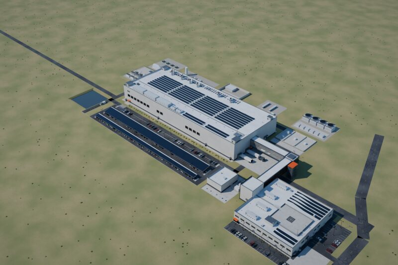
NAED Energy Holding Inc. has released engineering ratings for its proprietary PV-1 manufacturing line, detailing an operating throughput of 16,000 G12 half-cut wafers per hour per line for next-generation perovskite-silicon tandem solar cells, according to technical disclosures reported by CleanTechnica. Across a planned multi-line site configuration comprising six parallel units, the platform is designed to achieve an aggregate nameplate capacity of approximately 4.6 gigawatts annually, marking a significant engineering milestone in the push to transition tandem photovoltaic architectures from research environments to industrial high-volume production.
The commercialization of two-terminal perovskite-on-silicon tandem devices represents a pivotal technology shift for global clean technology markets and utility-scale solar developers currently pressing against the theoretical efficiency ceilings of standard monocrystalline silicon. By establishing an automated, vertical vacuum-coating methodology capable of high-cadence processing, NAED addresses the solar industry's central manufacturing dilemma: translating laboratory cell efficiencies into commercially viable, gigawatt-scale production runs without inflating capital costs or compromising device uniformity.
Engineering Architecture and Vacuum Integration
The PV-1 platform—designated PECVD-V—integrates plasma-enhanced chemical vapor deposition and physical vapor deposition processes onto a continuous, shared-carrier conveyor system. Production speed is anchored by an inline physical vapor deposition tool, designated ITO-1, which operates at a cycle rate of 400 wafers every 90-second machine index. To mitigate mechanical breakage and surface contamination on delicate thin films, substrates travel upright on edge within specialized vertical carriers throughout the deposition line.
A core mechanical innovation disclosed in the platform specifications is an automated, in-vacuum 180-degree carrier turnover mechanism. Inside the vacuum envelope, the system lifts and rotates the entire multi-wafer carrier to coat opposing faces of the substrate, eliminating the need for individual robotic wafer handling or substrate flipping. This continuous sequence maintains vacuum integrity, minimizes structural stress on the wafers, and ensures consistent deposition of critical charge-transport layers and transparent conductive oxides.
"Each PV-1 line is rated at 16,000 G12 half-cut wafers per hour: 400 wafers every 90-second index, a rate set by the line's inline PVD tool (ITO-1)," CleanTechnica reported, citing detailed technical specifications released by NAED.
Operational Metrics and Multi-Gigawatt Scaling
Under standard operational assumptions, each individual PV-1 production line delivers roughly 0.77 gigawatts of annual tandem cell manufacturing capacity. When scaled across the company's planned six-line site configuration, total factory throughput reaches 96,000 G12 half-cut wafers per hour, yielding between 4.6 GW and 4.7 GW of annualized nameplate output.
The production system is engineered specifically to manufacture NAED's proprietary T2X solar cell, a two-terminal tandem architecture that stacks a wide-bandgap perovskite top cell of approximately 1.7 electron volts directly onto a narrow-bandgap silicon heterojunction bottom cell of roughly 1.1 electron volts. This dual-junction configuration divides the solar spectrum, allowing the top cell to capture high-energy visible photons while the underlying silicon base absorbs longer infrared wavelengths, reducing thermalization losses.
While NAED's baseline factory planning benchmarks assume a conservative 30% cell conversion efficiency for economic modeling, internal optical and electronic simulations have indicated potential efficiencies reaching up to 34.4% for optimized T2X cell stacks. Achieving the nominal 30% baseline in commercial volume would offer utility-scale installations an efficiency premium of 5 to 7 percentage points over mainstream TOPCon and silicon heterojunction modules, materially reducing balance-of-system expenses including racking, land footprint, electrical balance, and structural installation labor.
Strategic Market Outlook and Commercial Hurdles
Despite the substantial throughput ratings disclosed by NAED, commercial deployment of tandem photovoltaics at multi-gigawatt scale faces significant operational hurdles. Chief among these is long-term field stability. While crystalline silicon cells routinely achieve 25-year to 30-year operational warranties under standard International Electrotechnical Commission testing protocols, metal-halide perovskite formulations must demonstrate sustained resilience against moisture ingress, thermal cycling, and continuous ultraviolet exposure in diverse field environments.
Capital markets and prospective module off-takers will closely monitor forthcoming qualification phases, including accelerated damp-heat testing, operational field-trial yields, and thermal endurance metrics. Furthermore, securing stable supply chains for specialized precursor chemistries, target materials for PVD sputtering, and vertical carrier assemblies will govern the commissioning timeline of NAED's multi-line infrastructure. If verified during initial commercial runs, NAED's high-speed vacuum transport platform could accelerate the deployment curve for tandem solar modules, exerting competitive pressure across international module supply chains.